If you want to use gates, you will need to learn something about their
physical characteristics. In this section we'll walk you through
wiring a simple gate circuit using one specific integrated circuit (IC)
the 7400 chip. It's a good introduction to some of the more complex
logic chips that you'll probably be using later.
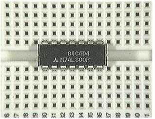
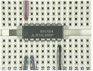
Here's a picture of the 7400 chip in a circuit
board. This chip is actually an N74LS00P. The LS
tells you that it is a low power Schottky chip. Every manufacturer
will embed the 7400 or 74LS00 in other part numbers.
Notice that this chip has fourteen pins.
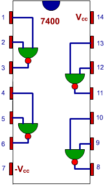
If you want to use an IC chip, then you will always need to know the pinout.
That's electrical engineering lingo for describing the way the pins are
connected to the internal circuitry of the chip. You need to know
where the power supply is connected and where the gate inputs and outputs
are connected. Here's the pinout for a 7400 chip.
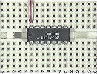
The first step in wiring the 7400 is to connect the positive power supply.
Use a five volt (5v) power supply and don't turn it on yet. Connect
a lead to pin 14 as shown below, and connect the other end of that lead
to a 5v supply. Keep the power supply turned off until you have everything
connected. Here's what that looks like when the positive supply voltage
to the chip is wired.
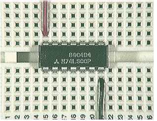
The next step in wiring the 7400 is to connect the ground connection.
Connect a lead to pin 7 as shown below, and connect the other end of that
lead to ground.
Notice the pattern to this connection. The power to this digital
logic chip goes to the corners. Remember, power
to the corners for logic chips.
Now you can connect the two inputs to one of the gates on the chip.
You're going to put 5v on either of these inputs for a 1
and ground the input for a 0.
There are two wires in the picture below that connect to pins 1 and 2 on
the chip. Those pins are the inputs for one of the NAND gates on
the chip.
Now you can connect the output of the gate. You will need to connect
this output to something like a voltmeter or an oscilloscope so that you
can measure and observe the output of the gate. (And the voltmeter
or oscilloscope will also have to be connected to the ground. You
will measure output voltage with respect to ground.) The output will
be near 5v when the output is a 1 and
near 0v when the output is a 0.
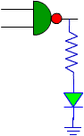
Actually, you can often connect LEDs to give a visual indication of a 1
(LED lighted) or a 0 (LED dark).
Here some LEDs are shown, together with 1kW current limiting resistors.
If you connect LED indicators to your circuit remember that an LED is not
the same in both directions, and you have to get the correct end connected
to the resistor. The other end of each LED is connected to ground
(or just "grounded"). Here's the circuit to show the output of a
NAND gate:
When the output of the gate is a 1,
the output voltage will be five (5) volts. Current will flow through
the series combination of the resistor and the LED, so the LED will light.
When the output of the gate is a 0,
the output voltage will be zero (0) volts and the LED will not be lit.
Thus, the LED lights up when the output is a 1,
and doesn't light when the output is a 0.
You can use this indication scheme to show the status for any signal.
(It doesn't have to be the output of a gate.)
Question
Q1
In the picture above, (shown again here) is the power turned on for the
chip power supply?
A
NAND Gate
Here is a photo of a NAND gate wired to display the input signals and output
signals. In this simulation you can manipulate the inputs and see
the inputs and outputs. Note the following.
The input voltage can
be set to either 5v or 0v (ground) for each input to one of the NAND gates
on the chip. Five volts is a logical 1, and zero volts is a logical
zero.
Note how the push buttons
move a connection from 5v to ground when the button is pushed.
When an signal is a 1,
there is an LED that lights to show that the input is 1. When the
LED is not lit, the signal is 0.
Note that there is a current
limiting resistor in series with each LED. If the voltage at the
output becomes 5v and the LED "saturates" around 1.8v, you need a current
limiting resistor. These resistors look to be 1kW
.
The power supply connection
and the ground connection to the chip are both shown. The vertical
line of connection points on the circuit board is ground.
Check out how the circuit works and note
all of the connections that you need to make to ensure that the chip works
as it is supposed to work.
Example
Problem
Let's reconsider the pump problem. What happens if there are times
when you don't want either pump to pump? Assume you have a digital
signal that is 1 when one of the two pumps
is to pump, and 0 when neither pump is to
pump. For example, if the pH was very close to desired you wouldn't
want to do anything at all so you wouldn't want either pump to turn on..
You still have the other signal that determines which pump is to pump whenever
one of the pumps should pump.
Devise a circuit that will ensure that both pumps are OFF when the Pumpsignal
is 0 and that the correct pump pumps when
the Pump signal is 1.
The circuit you devise in this section will be simple enough that you can
probably implement it with a few chips although you will need to look for
chips with AND gates and inverters. You should be able to handle
that now. Work through the solution in this lesson and try it out
in lab if you can.
Example Solution
Let's look at this problem with a truth table. Here's the truth table.
Pumps On
1 = ON
Pump Choice
0 = S
1 = W
Pump S
Pump W
0
0
0
0
0
1
0
1
0
0
2
1
0
0
1
3
1
1
1
0
In English, we say to turn Pump S (Strong reactant) ON when the pumps are
ON, and the strong reactant is chosen (Choice 3) and to turn Pump W (Weak
reactant) ON when the pumps are ON and the weak reactant is chosen (Choice
2). Otherwise, do nothing.
If we examine it closely we see that there is exactly one term in each
function. S is 1
only for choice 3, that is when you want PUMPS
ON and you want the strong reactant. Similarly, W
is 1 only for choice 2.
Here's the truth table again. Note the following:
We have defined Boolean
variables here for the various signals, P, C, S, and W.
We have indicated the
inputs by shading them green,
and the outputs by shading them orange.
P
C
S
W
0
0
0
0
0
1
0
1
0
0
2
1
0
0
1
3
1
1
1
0
Looking at the statement "S is 1 . . . when you want
Pumps ON AND
you want the strong reactant" then you can generate a logic expression
directly from the statement.
and also:
Finally, realize that it doesn't take much to implement these functions.
Note you only need one inverter and two AND
gates. Here's the circuit that turns the pumps on at the proper time.
This is an interactive simulation of the circuit, so you can toggle the
switches with the push buttons. Check it out.
Question
Q2 To
check out the circuit you should what?
A QUICK
QUESTION
Within the simulated circuit, determine the part of the circuit that genrates
a 1 when the
pumps are ON,
and a 0 when
they both are OFF.
What
If The Problem Isn't So Simple?
Not all functions are as simple as this one, and certainly not all can
be implemented with just a few gates. However, implementing this
simple function gives us a clue how to implement more complex functions.
In the next lesson we'll look at a more general method for implementing
functions - a method that uses only AND and OR gates and inverters - but
a method which can also be implemented with only NAND gates. We hope
that sounds intriguiging to you and that you are looking forward to the
next lesson.
Boolean
Algebra
Clearly at this point we are entering a realm of a different kind of algebra.
We have encountered some example terms in this algebra.
and:
The algebra is unusual because the variables in the algebra (S, P, C and
W in the example) can take only two values, 0 and 1. In this section
we will examine some of the properties of this algebra, and the implications
of what we have already learned.
There are some simple things we need to establish before we can proceed.
An AND
gate has this truth table when the inputs are A
and B, and the
output is C:
A
B
C
0
0
0
0
1
0
1
0
0
1
1
1
So, clearly we have:
0�0 = 0,
and
1�1 = 1,
and
0�1 = 0
Which
may be exactly what you expected.
We also need to consider an OR gate.
An OR
gate has this truth table when the inputs are A
and B, and the
output is C:
A
B
C
0
0
0
0
1
1
1
0
1
1
1
1
So, clearly we have:
0 + 0 = 0,
and
1 + 1 = 1,
and
0 + 1 = 1
Now,
if you are taking a college course, and you write home that 1 + 1 = 1 is
what you just learned, your parents may want your tuition refunded.
Now, if you accepted what was claimed above, then you also have to accept
the following:
A�A
= A
Just let A be either zero or one and remember
the truth table for an AND.
We also have:
A
+ A = A
Again, just let A be either zero or one and
remember the truth table for an OR.
And - - - believe it or not, this result for A + A is very useful because
it is a fundamental result that will let us build circuits with fewer gates.
We'll come back to that later.
There are some interesting theorems that can be proved. Note the
following:
These two little theorems will prove to be
useful. To prove these theorems you only need to know about the properties
of AND, OR and NOT gates. That is left as an exercise for you.
When we want to prove
a theorem we will take the approach that we can prove the theorem by examining
all possible combinations of the appropriate variables. We can do
that because the possible combinations are finite.
Here is a truth table. It lists all possible
combinations for two variables.
A
B
0
0
1
1
1
1
0
1
1
0
0
0
1
0
0
1
0
0
1
1
0
0
0
0
This truth table proves the following theorem.
Theorem
(de Morgan)
Proof
The proof of this theorem is contained in the truth table above which lists
every possible combination of A and B, and shows that this result is true.
One final note. There are some further simple facts that come in
useful. Note the following:
and:
Boolean Algebra can be a confusing and misleading business. De Morgan's
theorem above seems almost trivial. However, there is a very interesting
consequence of this theorem. Here it is:
If you have a Boolean
function that is a sum-of-products form it can be implemented using a two
layer circuit with the first layer composed of AND gates, and the second
layer composed of OR gates.
Applying deMorgan's theorem
to the function the circuit can be built using the same structure, but
replacing every AND and OR gate with a NAND gate.
First,
you need to understand how to expand a function in terms of minterms.