The bipolar junction transistor
The bipolar junction transistor is the cornerstone of much of today's
semiconductor electronics industry. This form of transistor has been in
existence for many years and is still very widely used in electronic circuits.
The bipolar transistor is very versatile and finds applications in many
applications and at a wide range of frequencies.
Beginnings ....
The bipolar transistor dates back to the middle of the twentieth century when
three scientists named Bardeen, Brattain, and Shockley working at Bell
Laboratories in the USA discovered it. They had been researching an idea for a
semiconductor field effect device, but they had been unable to make it work.
They had not succeeded in making this idea work and as a result they decided to
follow other lines of research and in doing this they developed the bipolar
transistor. They succeeded in making it work in late 1947, and only a week after
their initial discovery they demonstrated it in front of a group of executives
at Bell.
Today the semiconductor industry is enormous and vast quantities of money are
being invested in new semiconductor device developments. Although there are many
new types of transistor, the bipolar junction transistor is still in very
widespread use.
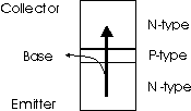
Structure
The bipolar transistor can be made from a variety of types of semiconductor. The
original devices were made from germanium, but silicon is widely used today.
In essence a transistor consists of an area of either p type of n type
semiconductor sandwiched between regions of oppositely doped silicon. As such
devices can be either a p-n-p or an n-p-n configuration.
There are three connections, namely the emitter, base, and the collector. The
base is the one in the centre and it is bounded by the emitter and collector. Of
the two outer two the collector is often made larger as this is where most of
the heat is dissipated.
The base derives its name from the first point contact transistors where the
centre connection also formed the mechanical "base" for the structure. It is
essential that this region should be as thin if high levels of current gain are
to be achieved. Often it may only be about 1 um across.
The emitter is where the current carriers are "emitted", and the collector is
where they are "collected".
Basic operation
The transistor can be considered as two p-n junctions that are placed back to
back. In operation, the base emitter junction is forward biased and the base
collector junction is reverse biased. When a current flows through the base
emitter junction, a current also flows in the collector circuit. This is larger
and proportional to the one in the base circuit. In order to explain the way in
which this happens, the example of an n-p-n transistor is taken. The same
principles are used for the p-n-p transistor except that the current carrier is
holes rather than electrons and the voltages are reversed.
Operation of a bipolar junction transistor
The emitter in the n-p-n device is made of n-type material and here the
majority carriers are electrons. When the base emitter junction is forward
biased the electrons move from the n-type region towards the p-type region and
the holes move towards the n-type region. When they reach each other they
combine enabling a current to flow across the junction. When the junction is
reverse biased the holes and electrons move away from one another resulting in a
depletion region between the two areas and no current flows.
When a current flows between the base and emitter, electrons leave the
emitter and flow into the base. Normally the electrons would combine when they
reach this area. However the doping level in this region is very low and the
base is also very thin. This means the most of the electrons are able to travel
across this region without recombining with the holes. As a result the electrons
migrate towards the collector, because they are attracted by the positive
potential. In this way they are able to flow across what is effectively a
reverse biased junction, and current flows in the collector circuit.
It is found that the collector current is significantly higher than the base
current, and because the proportion of electrons combining with holes remains
the same the collector current is always proportional to the base current. In
other words varying the base current varies the collector current.
The ratio of the base to collector current is given the Greek symbol B.
Typically the ratio B may be between 50 and 500 for a small signal transistor.
This means that the collector current will be between 50 and 500 times that
flowing in the base. For high power transistors the value of B is likely to be
smaller, with figures of 20 not being unusual.
Summary
The transistor is a current operated device. It is the amount of current flowing
in the base circuit that controls the amount of current flowing in the collector
circuit. The other major three terminal semiconductor device, the field effect
transistor is a voltage operated device. Here it is the potential on the gate
that controls the current passing between the source and drain.
|


