OneStopGate.Com
OnestopGate   OnestopGate
   Tuesday, April 30, 2024 Login  
OnestopGate
Home | Overview | Syllabus | Tutorials | FAQs | Downloads | Recommended Websites | Advertise | Payments | Contact Us | Forum
OneStopGate

GATE Resources
Gate Articles
Gate Books
Gate Colleges 
Gate Downloads 
Gate Faqs
Gate Jobs
Gate News 
Gate Sample Papers
Training Institutes

GATE Overview
Overview
GATE Eligibility
Structure Of GATE
GATE Coaching Centers
Colleges Providing M.Tech/M.E.
GATE Score
GATE Results
PG with Scholarships
Article On GATE
Admission Process For M.Tech/ MCP-PhD
GATE Topper 2012-13
GATE Forum


GATE 2025 Exclusive
Organizing Institute
Important Dates
How to Apply
Discipline Codes
GATE 2025 Exam Structure

GATE 2025 Syllabus
Aerospace Engg..
Agricultural Engg..
Architecture and Planning
Chemical Engg..
Chemistry
Civil Engg..
Computer Science / IT
Electronics & Communication Engg..
Electrical Engg..
Engineering Sciences
Geology and Geophysics
Instrumentation Engineering
Life Sciences
Mathematics
Mechanical Engg..
Metallurgical Engg..
Mining Engg..
Physics
Production & Industrial Engg..
Pharmaceutical Sciences
Textile Engineering and Fibre Science

GATE Study Material
Aerospace Engg..
Agricultural Engg..
Chemical Engg..
Chemistry
Civil Engg..
Computer Science / IT
Electronics & Communication Engg..
Electrical Engg..
Engineering Sciences
Instrumentation Engg..
Life Sciences
Mathematics
Mechanical Engg..
Physics
Pharmaceutical Sciences
Textile Engineering  and Fibre Science

GATE Preparation
GATE Pattern
GATE Tips N Tricks
Compare Evaluation
Sample Papers 
Gate Downloads 
Experts View

CEED 2013
CEED Exams
Eligibility
Application Forms
Important Dates
Contact Address
Examination Centres
CEED Sample Papers

Discuss GATE
GATE Forum
Exam Cities
Contact Details
Bank Details

Miscellaneous
Advertisment
Contact Us


Home » GATE Study Material » Electronics and Telecommunications » Electronic Components » Introduction to the PN junction and the basic diode

Introduction to the PN junction and the basic diode

Looking for GATE Preparation Material? Join & Get here now!

** Gate 2013 Question Papers.. ** CEED 2013 Results.. ** Gate 2013 Question Papers With Solutions.. ** GATE 2013 CUT-OFFs.. ** GATE 2013 Results.. **

Introduction to the PN junction and the basic diode

Semiconductor PN Junction

- the basis of the semiconductor diode

One of the fundamental structures within semiconductor technology is the PN junction. It is the fundamental building block of semiconductor diodes and transistors and a number of other electronic components. It has the valuable property that electrons only flow in one direction across it and as a result it acts as a rectifier. As it has two electrodes it receives its name - diode. In view of this, it is one of the most fundamental structures in semiconductor technology. Vast numbers of diodes are manufactured each year, and of course the PN junction is the basis of many other devices apart from diodes. The bipolar junction transistor, junction FET and many more all rely on the PN junction for their operation.


PN Junction


In its basic form a PN junction is formed from a piece of silicon by making one end P type and the other end N type. This means that both ends have different characteristics. One end has an excess of electrons whilst the other has an excess of holes. Where the two areas meet the electrons fill the holes and there are no free holes or electrons. This means that there are no available charge carries in this region. In view of the fact that this area is depleted of charge carriers it is known as the depletion region.

PN junction with no bias applied

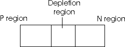
The semiconductor diode PN junction with no bias applied

Even though the depletion region is very thin, often only few thousandths of a millimetre, current cannot flow in the normal way. Different effects are noticed dependent upon the way in which the voltage is applied to the junction. If the voltage is applied such that the P type area becomes positive and the N type becomes negative, holes are attracted towards the negative voltage and are assisted to jump across the depletion layer. Similarly electrons move towards the positive voltage and jump the depletion layer. Even though the holes and electrons are moving in opposite directions, they carry opposite charges and as a result they represent a current flow in the same direction.

PN junction with forward bias applied

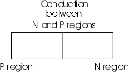
The semiconductor diode PN junction with forward bias

If the voltage is applied to the PN junction in the opposite sense no current flows. The reason for this is that the holes are attracted towards the negative potential that is applied to the P type region. Similarly the electrons are attracted towards the positive potential which is applied to the N type region. In other words the holes and electrons are attracted away from the junction itself and the depletion region increases in width. Accordingly no current flows.

PN junction with reverse bias

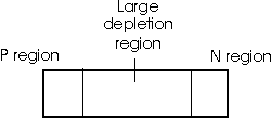
The semiconductor diode PN junction with reverse bias


Characteristics


The PN junction is not an ideal rectifier diode having infinite resistance in the reverse direction and no resistance in the forward direction.

PN junction diode characteristic

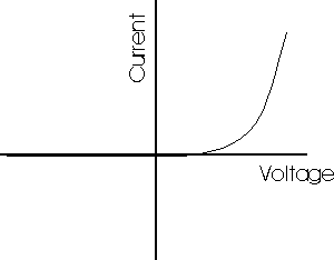
The characteristic of a diode PN junction

In the forward direction (forward biased) it can be seen that very little current flows until a certain voltage has been reached. This represents the work that is required to enable the charge carriers to cross the depletion layer. This voltage varies from one type of semiconductor to another. For germanium it is around 0.2 or 0.3 volts and for silicon it is about 0.6 volts. In fact it is possible to measure a voltage of about 0.6 volts across most small current diodes when they are forward biased. Power rectifier diodes normally have a larger voltage across them but this is partly due to the fact that there is some resistance in the silicon, and partly due to the fact that higher currents are flowing and they are operating further up the curve.

From the diagram it can be seen that a small amount of current flows in the reverse direction (reverse biased). It has been exaggerated to show it on the diagram, and in normal circumstances it is very much smaller than the forward current. Typically it may be a pico amps or microamps at the most. However it is worse at higher temperatures and it is also found that germanium is not as good as silicon.

This reverse current results from what are called minority carriers. These are a very small number of electrons found in a P type region or holes in an N type region. Early semiconductors has relatively high levels of minority carriers, but now that the manufacture of semiconductor materials is very much better the number of minority carriers is much reduced as are the levels of reverse currents.


Summary


Even though the basic diode PN junction may appear to have limited applications, it finds uses in a great variety of applications. Specialised versions of the diode are used for particular applications. The light emitting diode (LED) and photodiode are but two examples. However the PN junction is also the basis of the bipolar junction transistor, and the junction FET. There are also many many other examples of its use. As a result many billions of the PN junctions are manufactured each year, and it is the most fundamental structure to today's semiconductor electronics scene.


Discussion Center

Discuss/
Query

Papers/
Syllabus

Feedback/
Suggestion

Yahoo
Groups

Sirfdosti
Groups

Contact
Us

MEMBERS LOGIN
  
Email ID:
Password:

  Forgot Password?
 New User? Register!

INTERVIEW EBOOK
Get 9,000+ Interview Questions & Answers in an eBook. Interview Question & Answer Guide
  • 9,000+ Interview Questions
  • All Questions Answered
  • 5 FREE Bonuses
  • Free Upgrades
GATE RESOURCES
 
  • Gate Books
  • Training Institutes
  • Gate FAQs
  • GATE BOOKS
     
  • Mechanical Engineeering Books
  • Robotics Automations Engineering Books
  • Civil Engineering Books
  • Chemical Engineering Books
  • Environmental Engineering Books
  • Electrical Engineering Books
  • Electronics Engineering Books
  • Information Technology Books
  • Software Engineering Books
  • GATE Preparation Books
  • Exciting Offers


    GATE Exam, Gate 2009, Gate Papers, Gate Preparation & Related Pages


    GATE Overview | GATE Eligibility | Structure Of GATE | GATE Training Institutes | Colleges Providing M.Tech/M.E. | GATE Score | GATE Results | PG with Scholarships | Article On GATE | GATE Forum | GATE 2009 Exclusive | GATE 2009 Syllabus | GATE Organizing Institute | Important Dates for GATE Exam | How to Apply for GATE | Discipline / Branch Codes | GATE Syllabus for Aerospace Engineering | GATE Syllabus for Agricultural Engineering | GATE Syllabus for Architecture and Planning | GATE Syllabus for Chemical Engineering | GATE Syllabus for Chemistry | GATE Syllabus for Civil Engineering | GATE Syllabus for Computer Science / IT | GATE Syllabus for Electronics and Communication Engineering | GATE Syllabus for Engineering Sciences | GATE Syllabus for Geology and Geophysics | GATE Syllabus for Instrumentation Engineering | GATE Syllabus for Life Sciences | GATE Syllabus for Mathematics | GATE Syllabus for Mechanical Engineering | GATE Syllabus for Metallurgical Engineering | GATE Syllabus for Mining Engineering | GATE Syllabus for Physics | GATE Syllabus for Production and Industrial Engineering | GATE Syllabus for Pharmaceutical Sciences | GATE Syllabus for Textile Engineering and Fibre Science | GATE Preparation | GATE Pattern | GATE Tips & Tricks | GATE Compare Evaluation | GATE Sample Papers | GATE Downloads | Experts View on GATE | CEED 2009 | CEED 2009 Exam | Eligibility for CEED Exam | Application forms of CEED Exam | Important Dates of CEED Exam | Contact Address for CEED Exam | CEED Examination Centres | CEED Sample Papers | Discuss GATE | GATE Forum of OneStopGATE.com | GATE Exam Cities | Contact Details for GATE | Bank Details for GATE | GATE Miscellaneous Info | GATE FAQs | Advertisement on GATE | Contact Us on OneStopGATE |
    Copyright © 2024. One Stop Gate.com. All rights reserved Testimonials |Link To Us |Sitemap |Privacy Policy | Terms and Conditions|About Us
    Our Portals : Academic Tutorials | Best eBooksworld | Beyond Stats | City Details | Interview Questions | India Job Forum | Excellent Mobiles | Free Bangalore | Give Me The Code | Gog Logo | Free Classifieds | Jobs Assist | Interview Questions | One Stop FAQs | One Stop GATE | One Stop GRE | One Stop IAS | One Stop MBA | One Stop SAP | One Stop Testing | Web Hosting | Quick Site Kit | Sirf Dosti | Source Codes World | Tasty Food | Tech Archive | Software Testing Interview Questions | Free Online Exams | The Galz | Top Masala | Vyom | Vyom eBooks | Vyom International | Vyom Links | Vyoms | Vyom World
    C Interview Questions | C++ Interview Questions | Send Free SMS | Placement Papers | SMS Jokes | Cool Forwards | Romantic Shayari