OneStopGate.Com
OnestopGate   OnestopGate
   Monday, April 29, 2024 Login  
OnestopGate
Home | Overview | Syllabus | Tutorials | FAQs | Downloads | Recommended Websites | Advertise | Payments | Contact Us | Forum
OneStopGate

GATE Resources
Gate Articles
Gate Books
Gate Colleges 
Gate Downloads 
Gate Faqs
Gate Jobs
Gate News 
Gate Sample Papers
Training Institutes

GATE Overview
Overview
GATE Eligibility
Structure Of GATE
GATE Coaching Centers
Colleges Providing M.Tech/M.E.
GATE Score
GATE Results
PG with Scholarships
Article On GATE
Admission Process For M.Tech/ MCP-PhD
GATE Topper 2012-13
GATE Forum


GATE 2025 Exclusive
Organizing Institute
Important Dates
How to Apply
Discipline Codes
GATE 2025 Exam Structure

GATE 2025 Syllabus
Aerospace Engg..
Agricultural Engg..
Architecture and Planning
Chemical Engg..
Chemistry
Civil Engg..
Computer Science / IT
Electronics & Communication Engg..
Electrical Engg..
Engineering Sciences
Geology and Geophysics
Instrumentation Engineering
Life Sciences
Mathematics
Mechanical Engg..
Metallurgical Engg..
Mining Engg..
Physics
Production & Industrial Engg..
Pharmaceutical Sciences
Textile Engineering and Fibre Science

GATE Study Material
Aerospace Engg..
Agricultural Engg..
Chemical Engg..
Chemistry
Civil Engg..
Computer Science / IT
Electronics & Communication Engg..
Electrical Engg..
Engineering Sciences
Instrumentation Engg..
Life Sciences
Mathematics
Mechanical Engg..
Physics
Pharmaceutical Sciences
Textile Engineering  and Fibre Science

GATE Preparation
GATE Pattern
GATE Tips N Tricks
Compare Evaluation
Sample Papers 
Gate Downloads 
Experts View

CEED 2013
CEED Exams
Eligibility
Application Forms
Important Dates
Contact Address
Examination Centres
CEED Sample Papers

Discuss GATE
GATE Forum
Exam Cities
Contact Details
Bank Details

Miscellaneous
Advertisment
Contact Us


Home » GATE Study Material » Electronics and Telecommunications » Electronic Components » PIN Diode

PIN Diode

Looking for GATE Preparation Material? Join & Get here now!

** Gate 2013 Question Papers.. ** CEED 2013 Results.. ** Gate 2013 Question Papers With Solutions.. ** GATE 2013 CUT-OFFs.. ** GATE 2013 Results.. **

PIN Diode

The PIN diode

- for switching microwave, and photo diode applications

PIN diodes (p-i-n diodes) are used in many electronics applications, and in particular PIN diodes find uses in electronic switching applications. However it found its first applications in 1952 as a low frequency high power rectifier. The PIN diode is also used in a number of microwave applications, although it took until around 1960 before its use became more popular in this application. A further use is as a photo-detector (photodetector or photo-diode) where its structure is particularly suited to absorbing light.


Structure


The PIN diode consists of a semiconductor diode with three layers. The usual P and N regions are present, but between them is a layer of intrinsic material a very low level of doping. This may be either N-type or P-type, but with a concentration of the order of 13^13 cm^-3 which gives it a resistivity of the order of one k-ohm cm.

The thickness of the intrinsic layer is normally very narrow, typically ranging from 10 to 200 microns. The outer P and N-type regions are then heavily doped.

There are two ways in which the PIN diode can be realised. One is to fabricate the p-i-n diode in a planar structure, and the other is to use a mesa structure. When the planar structure is fabricated an epitaxial film is grown onto the substrate material and the P+ region is introduced either by diffusion or ion implantation. The mesa structure has layers grown onto the substrate. These layers have the dopants incorporated. In this way it is possible to control the thickness of the layers and the level of dopants more accurately and a very thin intrinsic layer can be fabricated if required. This is ideal for high frequency operation. A further advantage of the mesa structure is that it provides a reduced level of fringing capacitance and inductance as well as an improved level of surface breakdown.

PIN diode with a planar structure

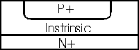
PIN diode with a planar construction

PIN diodes are widely made of silicon, and this was the semiconductor material that was used exclusively until the 1980s when gallium arsenide was introduced.


Characteristics


The main feature of the PIN diode is the intrinsic layer between the P-type and N-type regions. This enables it to provide properties such as a high reverse breakdown voltage, and a low level of capacitance. For microwave applications it offers carrier storage when it is forward biased.

It is found that at low levels of reverse bias the depletion layer become fully depleted. Once fully depleted the p-i-n diode capacitance is independent of the level of bias because there is little net charge in the intrinsic layer.

When the PIN diode is forward biased both types of current carrier are injected into the intrinsic layer where they combine. It is this process that enables the current to flow across the layer.

The particularly useful aspect of the PIN diode occurs when it is used with high frequency signals, the diode appears as a resistor rather than a non linear device, and it produces no rectification or distortion. Its resistance is governed by the DC bias applied. In this way it is possible to use the device as an effective RF switch or variable resistor producing far less distortion than ordinary PN junction diodes.


Applications


The PIN diode is used in a variety of different applications from low frequencies up to high radio frequencies. The properties introduced by the intrinsic layer make it suitable for a number of applications where ordinary PN junction diodes are less suitable.

In the first instance the diode can be used as a power rectifier. Here the intrinsic layer gives it a high reverse breakdown voltage, and this can be used to good effect in many applications.

Although the p-i-n diode finds many applications in the high voltage arena, it is probably for radio frequency applications where it is best known. The fact that when it is forward biased, the diode is linear, behaving like a resistor, can be put to good use in a variety of applications. It can be used as a variable resistor in a variable attenuator, a function that few other components can achieve as effectively. The PIN diode can also be used as an RF switch. In the forward direction it can be biased sufficiently to ensure it has a low resistance to the RF that needs to be passed, and when a reverse bias is applied it acts as an open circuit, with only a relatively small level of capacitance.

Another useful application of the PIN diode is for use in RF protection circuits. When used with RF, the diode normally behaves like a resistor when a small bias is applied. Hover this is only true for RF levels below a certain level. Above this the resistance drops considerably. Thus it can be used to protect a sensitive receiver from the effects of a large transmitter if it is placed across the receiver input.

PIN diode attenuattor and switch circuit

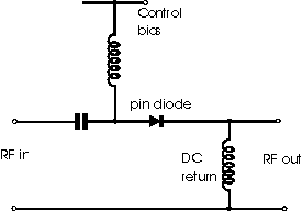
PIN diode attenuator and switch circuit

Finally the PIN diode finds many applications as a photodiode, although this will be explained separately.


Discussion Center

Discuss/
Query

Papers/
Syllabus

Feedback/
Suggestion

Yahoo
Groups

Sirfdosti
Groups

Contact
Us

MEMBERS LOGIN
  
Email ID:
Password:

  Forgot Password?
 New User? Register!

INTERVIEW EBOOK
Get 9,000+ Interview Questions & Answers in an eBook. Interview Question & Answer Guide
  • 9,000+ Interview Questions
  • All Questions Answered
  • 5 FREE Bonuses
  • Free Upgrades
GATE RESOURCES
 
  • Gate Books
  • Training Institutes
  • Gate FAQs
  • GATE BOOKS
     
  • Mechanical Engineeering Books
  • Robotics Automations Engineering Books
  • Civil Engineering Books
  • Chemical Engineering Books
  • Environmental Engineering Books
  • Electrical Engineering Books
  • Electronics Engineering Books
  • Information Technology Books
  • Software Engineering Books
  • GATE Preparation Books
  • Exciting Offers


    GATE Exam, Gate 2009, Gate Papers, Gate Preparation & Related Pages


    GATE Overview | GATE Eligibility | Structure Of GATE | GATE Training Institutes | Colleges Providing M.Tech/M.E. | GATE Score | GATE Results | PG with Scholarships | Article On GATE | GATE Forum | GATE 2009 Exclusive | GATE 2009 Syllabus | GATE Organizing Institute | Important Dates for GATE Exam | How to Apply for GATE | Discipline / Branch Codes | GATE Syllabus for Aerospace Engineering | GATE Syllabus for Agricultural Engineering | GATE Syllabus for Architecture and Planning | GATE Syllabus for Chemical Engineering | GATE Syllabus for Chemistry | GATE Syllabus for Civil Engineering | GATE Syllabus for Computer Science / IT | GATE Syllabus for Electronics and Communication Engineering | GATE Syllabus for Engineering Sciences | GATE Syllabus for Geology and Geophysics | GATE Syllabus for Instrumentation Engineering | GATE Syllabus for Life Sciences | GATE Syllabus for Mathematics | GATE Syllabus for Mechanical Engineering | GATE Syllabus for Metallurgical Engineering | GATE Syllabus for Mining Engineering | GATE Syllabus for Physics | GATE Syllabus for Production and Industrial Engineering | GATE Syllabus for Pharmaceutical Sciences | GATE Syllabus for Textile Engineering and Fibre Science | GATE Preparation | GATE Pattern | GATE Tips & Tricks | GATE Compare Evaluation | GATE Sample Papers | GATE Downloads | Experts View on GATE | CEED 2009 | CEED 2009 Exam | Eligibility for CEED Exam | Application forms of CEED Exam | Important Dates of CEED Exam | Contact Address for CEED Exam | CEED Examination Centres | CEED Sample Papers | Discuss GATE | GATE Forum of OneStopGATE.com | GATE Exam Cities | Contact Details for GATE | Bank Details for GATE | GATE Miscellaneous Info | GATE FAQs | Advertisement on GATE | Contact Us on OneStopGATE |
    Copyright © 2024. One Stop Gate.com. All rights reserved Testimonials |Link To Us |Sitemap |Privacy Policy | Terms and Conditions|About Us
    Our Portals : Academic Tutorials | Best eBooksworld | Beyond Stats | City Details | Interview Questions | India Job Forum | Excellent Mobiles | Free Bangalore | Give Me The Code | Gog Logo | Free Classifieds | Jobs Assist | Interview Questions | One Stop FAQs | One Stop GATE | One Stop GRE | One Stop IAS | One Stop MBA | One Stop SAP | One Stop Testing | Web Hosting | Quick Site Kit | Sirf Dosti | Source Codes World | Tasty Food | Tech Archive | Software Testing Interview Questions | Free Online Exams | The Galz | Top Masala | Vyom | Vyom eBooks | Vyom International | Vyom Links | Vyoms | Vyom World
    C Interview Questions | C++ Interview Questions | Send Free SMS | Placement Papers | SMS Jokes | Cool Forwards | Romantic Shayari