The Schottky barrier diode
- a summary or tutorial of the basics of the Schottky Barrier Diode
The Schottky diode or Schottky Barrier diode is an
electronics component that is widely used for radio frequency (RF) applications
as a mixer or detector diode. The Schottky diode is also used in power
applications as a rectifier, again because of its low forward voltage drop
leading to lower levels of power loss compared to ordinary PN junction diodes.
Although normally called the Schottky diode these days, named after Schottky, it
is also sometimes referred to as the surface barrier diode, hot carrier or even
hot electron diode.
Despite the fact that Schottky barrier diodes have many
applications in today's high tech electronics scene, it is actually one of the
oldest semiconductor devices in existence. As a metal-semiconductor devices, its
applications can be traced back to before 1900 where crystal detectors, cat's
whisker detectors and the like were all effectively Schottky barrier diodes.
Structure
The Schottky barrier diode can be manufactured in a variety
of forms. The most simple is the point contact diode where a metal wire is
pressed against a clean semiconductor surface. This was how the early Cat's
Whisker detectors were made, and they were found to be very unreliable,
requiring frequent repositioning of the wire to ensure satisfactory operation.
In fact the diode that is formed may either be a Schottky barrier diode or a
standard PN junction dependent upon the way in which the wire and semiconductor
meet and the resulting forming process.
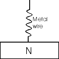
Point contact Schottky diode
Although point contact diodes were manufactured many years
later, these diodes were also unreliable and they were subsequently replaced by
a technique in which metal was vacuum deposited.
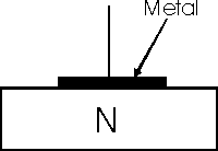
Deposited metal Schottky barrier diode
One of the problems with the simple deposited metal diode is
that breakdown effects are noticed around the edge of the metalised area. This
arises from the high electric fields that are present around the edge of the
plate. Leakage effects are also noticed. To overcome these problems a guard ring
of P+ semiconductor fabricated using a diffusion process is used along with an
oxide layer around the edge. In some instances metallic silicides may be used in
place of the metal.
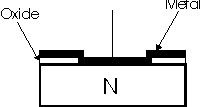
Deposited metal and oxide film Schottky diode
There are a number of points of interest from the fabrication
process. The most critical element in the manufacturing process is to ensure a
clean surface for an intimate contact of the metal with the semiconductor
surface, and this is achieved chemically. The metal is normally deposited in a
vacuum either by the use of evaporation or sputtering techniques. However in
some instances chemical deposition is gaining some favour, and actual plating
has been used although it is not generally controllable to the degree required.
When silicides are to be used instead of a pure metal
contact, this is normally achieved by depositing the metal and then heat
treating to give the silicide. This process has the advantage that the reaction
uses the surface silicon, and the actual junction propagates below the surface,
where the silicon will not have been exposed to any contaminants. A further
advantage of the whole Schottky structure is that it can be fabricated using
relatively low temperature techniques, and does not generally need the high
temperature steps needed in impurity diffusion.
Characteristics
The Schottky diode is what is called a majority carrier
device. This gives it tremendous advantages in terms of speed because it does
not rely on holes or electrons recombining when they enter the opposite type of
region as in the case of a conventional diode. By making the devices small the
normal RC type time constants can be reduced, making these diodes an order of
magnitude faster than the conventional PN diodes. This factor is the prime
reason why they are so popular in radio frequency applications.
The diode also has a much higher current density than an
ordinary PN junction. This means that forward voltage drops are lower making the
diode ideal for use in power rectification applications.
Its main drawback is found in the level of its reverse
current which is relatively high. For many uses this may not be a problem, but
it is a factor which is worth watching when using it in more exacting
applications.
The overall I-V characteristic is shown below. It can be seen
that the Schottky diode has the typical forward semiconductor diode
characteristic, but with a much lower turn on voltage. At high current levels it
levels off and is limited by the series resistance or the maximum level of
current injection. In the reverse direction breakdown occurs above a certain
level. The mechanism is similar to the impact ionisation breakdown in a PN
junction.
Applications
The Schottky barrier diodes are widely used in the
electronics industry finding many uses as a general purpose rectifier. However
they has come into their own for radio frequency applications because of their
high switching speed and high frequency capability. In view of this Schottky
barrier diodes are used in many high performance diode ring mixers. In addition
to this their low turn on voltage and high frequency capability and low
capacitance make them ideal as RF detectors.
Schottky barrier diodes are also used in high power
applications, as rectifiers. Their high current density and low forward voltage
drop mean that less power is wasted than if ordinary PN junction diodes were
used. This increase in efficiency means that less heat has to be dissipated, and
smaller heat sinks may be able to be incorporated in the design.
Schottky barrier diodes may also be used as a clamp diode in
a transistor circuit to speed the operation when used as a switch. They were
used in this role in the 74LS (low power Schottky) and 74S (Schottky) families
of logic circuits. Schottky barrier diodes are inserted between the collector
and base of the driver transistor to act as a clamp. To produce a low or logic
"0" output the transistor is driven hard on, and in this situation the base
collector junction in the diode is forward biased. When the Schottky diode is
present this takes most of the current and allows the turn off time of the
transistor to be greatly reduced, thereby improving the speed of the circuit.
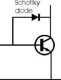
An NPN transistor with Schottky diode clamp
Schottky barrier diodes are also used as a fundamental
building block in a number of other devices from photodiodes to MESFETs. Not
only do Schottky barrier diodes find widespread use in many applications in its
own right, but it an essential part of many other components as well. As a
result the Schootky barrier diode is likely to remain in use for many years to
come.
|


